Back to top
Learn Advanced Debugging Techniques for High-Speed SERDES Designs
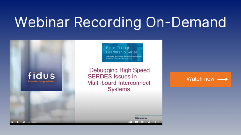
WEBINAR RECORDING ON-DEMAND
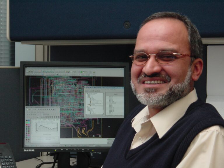
In this insightful session led by Dr. Syed Bokhari, a renowned Signal Integrity Architect from Fidus Systems, learn advanced techniques for improving signal integrity in high-speed SERDES, focusing on S-Parameter Analysis and FPGA Debugging, to address the challenges of electromagnetic interference and ground plane resonance accurately.
- Title: Debugging High Speed SERDES Issues in Multi board Interconnect Systems
- Speaker: Dr. Syed Bokhari, Signal Integrity Architect, Fidus Systems
- Date Published: January 19, 2024
- Duration: 55 Minutes
Overview
In the fast-paced world of high-speed digital designs, Signal Integrity Architect Dr. Syed Bokhari of Fidus Systems with over two decades of experience, dives deep into the complexities of debugging high-speed SERDES designs. From exploring common issues to providing practical solutions, this webinar covers crucial aspects like signal integrity, PCB design optimizations, FPGA testing techniques, and much more. Whether you’re dealing with millimeter-wave frequency challenges, coaxial cable impedance, or ground plane resonance, this session offers invaluable insights and real-world examples to enhance your high-speed applications.
Key Insights

- Understanding Signal Integrity in High-Speed SERDES: Detailed examination of how signal integrity issues manifest in high-speed SERDES designs, emphasizing the importance of accurate modeling and simulation to predict and mitigate potential problems.
- Electromagnetic Challenges in SERDES: Bokhari initiated the conversation by highlighting the electromagnetic nature of high-speed SERDES problems, particularly at millimeter-wave frequencies. These challenges necessitate a shift from traditional circuit analysis to a more comprehensive electromagnetic perspective.
- The Critical Role of Ground Plane Resonance: A significant portion of the webinar was dedicated to understanding ground plane resonance — a common yet often overlooked issue that can severely impair signal integrity. Dr. Bokhari outlined methods to detect and mitigate such resonance, ensuring stable and reliable data transmission.
- FPGA-Based Debugging Techniques: Leveraging FPGAs for debugging emerged as a potent strategy, thanks to their flexibility in simulating various data rates and patterns. This section provided attendees with actionable techniques to identify and address signal integrity issues efficiently.
- Case Study on QSFP Module Troubleshooting: Through a detailed case study, Dr. Bokhari walked the audience through the process of diagnosing and resolving errors in Quad Small Form-factor Pluggable (QSFP) modules, emphasizing systematic analysis and targeted interventions.
- S-Parameter Analysis for Accurate Impedance Matching: The webinar underscored the importance of S-parameter analysis in ensuring accurate impedance matching throughout the SERDES path. Attendees gained insights into utilizing S-parameters for predicting and optimizing system performance.
- Discrepancies Between Simulation and Reality: A critical discussion on the limitations of numerical simulations revealed the potential for discrepancies between simulated outcomes and real-world performance, prompting a call for rigorous validation and testing protocols.
- Navigating Complex SERDES Issues with Advanced Tools and Methodologies: Dr. Bokhari concluded with an overview of advanced tools, including 3D electromagnetic simulation, that are crucial for uncovering and solving complex SERDES design issues not readily apparent in circuit-level analyses.
- Interactive Q&A Session: Insights from the live Q&A session, where participants engaged with Dr. Bokhari on topics ranging from low-cost PCB material use in high-speed applications to the prioritization of test parameters in long-reach SERDES applications, enriching the webinar with diverse perspectives and expert advice.
Feedback and Further Questions:
For those who have additional inquiries or require further clarification on topics discussed during the webinar, please reach out to our technical team.
Additional Resources

- Stay informed about upcoming webinars in our Thought Leadership Series by joining our upcoming webinars. Visit our webinar series page for more information and registration details.
- Learn about debugging high-speed SERDES issues in multi-board interconnect systems by reading Dr. Syed Bokhari’s article.
- Register for an upcoming distinguished lecturer talk organized by Dr. Syed Bokhari on “Well Stirred is Half Measured: EMC Tests in Reverberation Chambers”.
Webinar Transcript
[00:00] Welcome and brief introduction by Mike McCarthy. Highlights on webinar logistics, recording availability, and Q&A procedures.
Everyone, we will give it just one more minute before we start the webinar.
Okay, let’s get started. Thank you, everyone, for attending our webinar in the Fidus Thought Leadership Series of webinars. My name is Mike McCarthy. I’ll be taking just a few seconds to cover some administrative stuff. We will be recording this webinar, and we will send a recording out to everyone after the webinar. If you have questions about the topic, please feel free to post them in the questions area. I will be actively monitoring the questions. If appropriate, I’ll ask them during the webinar, or we’ll also have some time at the conclusion of the webinar to address those questions. If we do run out of time, we will follow up with any additional questions in a follow-up email after the webinar has been completed.
[3:43] Introduction of Dr. Syed Bokhari, a signal integrity architect at Fidus with over 20 years of experience. Overview of his expertise and contributions to the field.
Now, it’s my pleasure to introduce our speaker today, Dr. Syed Bokhari, who serves as a Signal Integrity Architect at Fidus, where he has worked for over 20 years. He holds a doctorate in engineering, specializing in numerical electromagnetics, and is the chairman of the IEEE Ottawa EMC chapter. His area of research interests includes signal and power integrity, EMC, numerical methods in electromagnetics, and miniaturized antennas. He has many publications in these areas and holds two patents. I would now like to turn over the floor to Saeed for his presentation. Thank you.
[04:25] Overview of the webinar’s focus on high-speed SERDES designs, common issues, and debugging strategies. Introduction of a thought-provoking question about coaxial cable impedance.
Thank you, Mike. And thank you, everyone, for taking the time to attend this presentation. As Mike mentioned, as a part of our Fidus Thought Leadership Series, the topic we have chosen for this presentation is incredibly useful for hardware designers and signal integrity engineers who deal with high-speed SERDES designs. Those of us who have designed or used SERDES typically are talking about data rates of SERDES in the range from Now PCIe Gen three at eight gigabits per second going all the way up to the highest speeds. Levels like 25 gigabits per second are quite common today. In this entire range, there are issues that can range from something as simple as a high bit error rate all the way to complete catastrophic failure. What I’m presenting today is how one goes about debugging a high-speed SERDES problem. We are used to doing things in a certain way, simply to making our tasks easier. As a result, we use simplifications and approximations. The frequencies that we deal with for SERDES are actually in the millimeter-wave range at 25 gigabits per second, 30 gigabits per second. It has a Nyquist frequency of about 12 and a half gigahertz, and if you cover up to three to four times the Nyquist frequency, we are well into the millimeter-wave range. So, these problems are essentially electromagnetic problems that we are solving, but we do make things convenient. We reduce these electromagnetic field problems into circuit problems where we need to deal with voltages and currents, which is what we can measure. So, in this process, we end up making approximations. And one of the highlights of this presentation is questioning some of those approximations.
[06:38] Detailed exploration of the challenges in designing high-speed SERDES systems, including data rates, signal integrity issues, and the simplifications used in design processes.
So, I will be presenting two practical examples that involve actual designs which have been measured as well as simulated, to prove the point of how certain approximations can affect the performance of SERDES.
Before I start with the presentation, just to get a sense and to understand how one perceives the problem, I’ll start with a simple question.
[07:16] The Coaxial Cable Question: Understanding Initial Perceptions
See this. Okay, there you go. The question is intentionally vague because we just want to know what your immediate reaction to this question might be. If I have two 50-ohm coaxial cables and connect them together, will the impedance of the new cable be 50 ohms? The question doesn’t give you a lot of detail, but we’re interested in your knee-jerk reaction. Just make a note of what your answer is, and then we’ll discuss it at the end to see what the right answer could be. Some of you may say yes, thinking, “If two 50-ohm coaxial cables are connected together, what else could it be?” Some of you may choose to say no for some reason. And a neutral answer, which in signal integrity always uses that maybe, becomes an “It depends.” There’s never a definite answer. So, for a quick question like this, you can have multiple answers.
[08:35] Rephrasing the Question for Clarity
To rephrase the question into something different, for example, like this: If I gave you two S-parameter files of two different 50-ohm coaxial cables, could you run a simulation and tell me if the impedance of the new cable would be 50 ohms? When phrased in this way, it is very easy to take these S-parameter files – one S-parameter file corresponding to a 50-ohm cable, connect it to the other file, cascade them, and if you run any simulator, it will give you a 50-ohm result.
[09:17] Simulation vs. Reality: Exploring Different Outcomes
So, the answer from a simulation will always be 50 ohms, regardless of any conditions, because that’s how the numerical simulation is done. But now, let’s go back and see what the various answers may have come from and what is the reasoning behind the yes, no, or maybe.
Those of you who may have said yes would probably assume that the cables are identical. If you take two identical cables of the same diameter, physical dimensions, and connect them together, the end result will be 50 ohms. There’s no question about that. So, those of you who may have said no probably imagine that coaxial cables come in various diameters; some thick, some thin. And if you connect a thick cable with a thin cable, you do have a discontinuity at that point of connection, and that can lead to an impedance that is not 50 ohms. So, the answer would be no, it cannot be 50 ohms. And obviously, if you went a little more deeply into this thinking, saying, “How do I connect a thinner cable to a thicker cable?” They must use an adapter. If you use an adapter, adapters are generally frequency-dependent, and for this reason, you will probably get 50 ohms up to a certain frequency, and beyond that frequency, it may no longer be 50 ohms.
[10:52] Emphasizing the Difference Between Simulation and Reality
So, the point to make here is that simulation will always give one answer, but reality could be three different situations that we are trying to model, which could be different. That is one point to note. The second point is dealing with these high-speed SERDES; we are talking about millimeter-wave frequencies. At these frequencies, most, if not all, the structures we deal with are radiative, and these are like antennas. And that’s why I’ve taken an example of a microstrip patch antenna. The antenna is a rectangular patch; it’s a metallic patch of rectangular shape. There is a ground plane, which could represent a PCB, and the antenna is excited at one location, usually along a symmetric axis, off centered. It could be. We will insert a ground wire at some point to connect the rectangular-shaped patch to the ground plane underneath it. If we measure the input impedance of this antenna as a function of frequency, we will see a result like this: it will have a real and imaginary part. At certain frequencies, it will go through a resonance where the reactance goes from inductive to capacitive, and the resistance also increases. A typical microstrip patch antenna has a resonant frequency when its linear dimension is about a half-guide wavelength, that’s about 1.3 gigahertz here for the dimensions I have chosen, and you will see multiple resonances at the integral multiples of that resonant frequency, the second resonance here.
This is the normal operation of an antenna, a robust antenna. If I make a small change and insert just one ground wire at a corner of this rectangular patch, something entirely different happens: the resonant frequency drops from 1.3 gigahertz to literally a quarter of the value, and this is actually a way to design miniaturized antennas. The point here to note is that one single ground wire at a precise location can make the resonant frequency move by a factor of four. And certain resonances will be absent when you have ground vias on the patch.
So, in reality, this patch represents a power plane on a PCB; it could be anything else with a shape, and the ground plane is the large ground plane on a PCB, which is connected by decoupling capacitors to the power planes or just a ground shape, a floating ground shape, which is connected by ground vias. So, just by having a few ground vias connected to a large ground plane, you can actually change the resonant frequency by a large amount. The takeaway message from that question I had is that while the nice, simplified S parameters of cascaded networks are exact in a circuit sense, you can cascade S parameters, but in an electromagnetic sense, it is an approximation, and you need to know what it represents so that you can ensure you’re not applying an electromagnetic problem to a circuit problem blindly. This is an important thing to keep in mind, and oftentimes, it is possible to do that.
The second thing to remember is that ground plane layers, ground planes, power planes, these all have high-Q resonances. The frequencies at which you have complex behavior due to geometry and ground via allocation, resonances are present all the time; it’s a question of whether they get excited. If the resonance does get excited with sufficient energy, then it can cause a lot of trouble.
[15:25] Starting the Presentation: Designing a High-Speed Backplane System
So, with these two points in mind, let’s actually start the presentation now and dive into the examples. In this presentation, we deal with a typical example of designing a high-speed backplane system. This applies to any SERDES where a SERDES might be running. So, we may have gone through an exercise of optimization; we would model the via separately, maybe just to keep the computation time small. Pick a few nets, typically three, to improve crosstalk through some kind of optimization. Include connectors in the path, include traces, optimize anti-pads, set up these various elements, blocks, simulate them separately, include the manufacturer-specified data where available, and construct a circuit diagram like what I’ve shown here. Then, once the link is established, these are S-parameter blocks that are concatenated. Some of these we might want to introduce a pin skew in the differential pairs by adding a transmission line to represent the fiber weave skew. And we would compute the insertion loss of the whole link, maybe run it through an eye diagram simulation to obtain a result.
[16:53] Understanding S-Parameter Blocks and Ground References
Now, just pay attention to this slide, and then I’m going to show you the next one. Okay, these two slides are literally identical, but they have a small difference. The difference, as you can see, is that each of these blocks, S-parameter blocks, has its own ground reference, which is when we determine the parameters of a block, we don’t know exactly what it connects to. But it has its own ground reference. When you hook them up together, here we are actually hooking up the grounds as well, although we don’t see it very clearly in a schematic like this. We assume that the grounds are also connected exactly, and this is where the assumption is very critical.
[17:42] Identifying Common SERDES Issues
So, let’s now see what the kinds of SERDES issues are that one encounters normally. So, we say a common problem is that the multi-board system has an unacceptable bit error rate at, say, 25 gigabits per second. Which means that the error rate has exceeded the 10^-14 or some metric that you’re trying to hit; this is a common problem. And then the solution is to find out why it is so. In safe conditions, the bit error rate can be improved or just brought down to zero, as much as possible. So, I have an example of this.
[18:31] Exploring Specific SERDES Challenges
Now, the second example is that the system works at 10 gigabits per second but fails to operate in the extended mode for 10GBase-KR. This is a very common scenario where you may have seen the system works at one speed but not at a slightly higher speed. This could indicate that the design has a low margin, which is why just increasing the data rate by a small amount causes it to fail. Often, if you want to use the same system to run at the next generation (like PCI Express Generation 3 to Generation 4), it might not be possible if the previous generation didn’t have a lot of margin.
Another complex issue is when eight out of ten boards appear to run error-free. This could indicate board-to-board variation, possibly due to fiber weave effects. These are the real challenges: all lanes except two run error-free at 25 gigabits per second, which is extremely hard to debug because if everything looks almost the same, why do two lanes fail? This scenario is real and puzzling. It might even seem funny, but it’s true that sometimes a system seems to work fine when you press hard on the connector. For those who have worked with QSFP modules, try slightly retracting the module in the lab and observe what happens to the errors. They can sometimes get better or worse. And then, some might give up on finding the root cause, assuming it’s due to missing ground planes or too many split power planes being used. Adding a lot of ground vias can sometimes make the problem go away. So, we can encounter any or all of these combinations of SERDES issues. In reality, finding solutions for the first type of problems might be simpler, mostly a margin issue. However, the last category, those highlighted in red, are usually very hard to debug.
[19:25] Theoretical Framework and Signal Integrity Parameters
And we’ll present here a theory that can explain why sometimes you see these variations. Now, when we, when we design, this, just a refresher, a quick refresher on, on the parameters of interest, yes, parameters that we deal with are typically, you have a skew between the P and N, defense, we highlight that as being very critical, it is not a fundamental parameter, but it affects all the fundamental parameters. The most fundamental one we would consider, is the insertion loss, insertion loss is the energy that’s lost over the link, then you have return loss, which is the reflected, reflected energy. And then you have crosstalk, which comes in two types, usually the far-end crosstalk and the near-end crosstalk, this would be identified as the fundamental S parameters, and IEEE has, IEEE has specifications on these, on what they are.
Now, in this diagram, we try to simplify them. So, in a system, almost everything affects the skew, which is the fundamental parameter, the PCB material, traces are, cannot, can never be straight, they have to bend, they contribute to skew, vias contribute to skew, can contribute to skew, you have capacitors, sometimes on the differential pairs, they need, are identical, exactly identical, they can contribute to skew, the breaking out of the traces near the BGA region can, we will, is never identical, so that, they can, that can result in a skew. Almost all connectors will have some amount of skew in them. And you have the stack-up as well, which can cause skew because the material, any of these things, and all of these will affect the fundamental parameters, insertion loss, return loss.
[23:35] Design and Debugging Flowchart
Now, with these, to an end, the crosstalk, once we use the crosstalk, we define an insertion loss to Crosstalk ratio. And the insertion loss variation is also specified as an insertion loss deviation. So, these are the parameters that the IEEE, for example, 10 G base carrier, used in the beginning, they still continue to use this, although there are a few more, more reward ones, such as common, effective return loss, these days, yet the fundamental ones remain the same, okay. So, we would usually use a flowchart to design, and while debugging, we just use the same flowchart, and then go backwards. So, just see if everything is met. Typically, this is when you’re dealing with a long link, and it’s almost always the case in high-speed SERDES. You are, your frequency of interest is primarily what we call the Nyquist frequency, which is, for, it’s really just half the data rate. So, 25 gigabits per second, we’re looking at, at 12 and a half gigahertz, Nyquist frequency. We look at the parameters at this frequency because the link is long. The end, even if a pulse is transmitted, it will look like a sine wave eventually, and so, it is good enough to deal with the Nyquist frequency. The first Nyquist frequency, sometimes we may want to go up to two to three times Nyquist, was quite rare. So, at that frequency, we calculate the insertion loss. And we can check and see if the, the silicon devices that are used can transmit this amount of energy and receive it as well. If they cannot, then you probably use a retimer or redriver in the circuit, and then go through all the other IEEE requirements, to see if they’re satisfied, then maybe do an eye diagram simulation, to some optimization, and that gives us a link, a link that could meet an error-free operation.
[25:44] Signal Integrity Testing and Troubleshooting
So, when we have a problem, it is possible that if there is a problem where the devices can, the data rate of the devices can be changed. And this is especially true when we are using FPGAs. When you’re using FPGAs, the data rate can, drop, can be varied, we could find out if, if the device, if a link does not operate at 25 gigabits per second, does it operate at a lower speed, lower data rate? Maybe 16? Or maybe less? That is already an indication that there’s a signal integrity problem.
[26:24] Advanced Testing and Problem Solving with FPGAs
Now, another test would be, where it’s possible, again with FPGAs, can you operate with a lower pseudo-random bit stream, like, say, PRBS seven pattern, and does it work error-free, or that, with that pattern, the pattern also determines the bit, the frequency, or bit variation. And that’s another test to do. And another test, very useful test to do, where it’s possible, is to enable and disable lanes selectively. Now, if we have a number of lanes, and we disable all except one, and then the operation is, the, is robust. And then, as soon as we turn on another lane, it starts giving errors, then we know that there is a crosstalk effect. These are easy to debug when the devices used are FPGAs because they invariably provide these, a variable, at a variable data rate, Variable Data pattern capability, and the ability to enable and disable lanes. But, in general, it is not, it’s not possible.
[27:28] Case Study: QSFP Modules and Signal Integrity
So, let’s start with the problem. That’s the standard application involving QSFP modules. It could be an FMC type of application, where you have a large board with a number of ASICs or FPGAs that are hooked up through a connector to a number of QSFP modules, let’s say, a number of them, they might be running at a 25 G carry, in which case, we also have a, in, session, precise, determining session, and in, session loss budgets, 10 DB or something, in this case. So, here, a common problem is, again, errors appearing on one or more of these QSFP modules. So, there’s one problem, which we debug here, we did a measurement, actually, with a system that had similar, to how the system worked, where it had lots of errors.
So, when we simulated and measured the link from end to end, we saw that it was exceeding that 10 DB insertion loss requirement by about three dB, and it also had a very high return loss, at the fundamental frequency, look at the return loss, it is almost, like dB down, so it is extremely high. And as a result of this poor return loss, he also, we also got a very bad, in, session loss deviation, if you see this, the way, this, the insertion loss curve is, it should ideally be a straight line, the way it is oscillating, it increased the insertion loss deviation. So, the result was, and I, that is very marginal, and which is clearly what, right to bid bidders. So, the solution, in this case, was to use a better PCB material, and improve on the insertion loss, and do some optimization to improve on the return loss, it was not possible to do the optimization to the fullest extent. And so, we ended up with some improvement on the insertion loss, by using higher quality material. But the return loss was marginally improved. And with this, once we simulated it, you can see that the eye diagram, the eye opens up very nicely. And it passed, this lens, all those failing, the high error data lens gave error, was rendered error-free. So, fairly easy. A relatively easier problem to, to debug, and determine, say, question of high insertion loss deviation, and not meeting the margin. Now, now, we will talk about the more, the more interesting, the critical problem, the problem where the answer is not very obvious.
[30:18] Exploring the Impacts of Ground Plane Resonance through Simulation and Measurement
So, when we cascade networks, we make the implicit assumption that the reference, reference plane, the ground reference, ground, is, of both cascaded, of both parts of the network, is, has a very low impedance connection. This, this, this connection is implied, and we see the impact of this in the, in the next example that I showed.
[30:52] Practical Example: Air Dielectric and Copper Pieces
So, here’s an example of a very simple structure. But, just mostly, to prove the point. So, I have air dielectric; I don’t want to complicate anything here; we have two rectangular pieces of copper, A, three axis, three, the, matches, is a wide-shaped rectangle, piece of copper, B, is a very thin and narrow strip. And C is almost identical to A, but with an, except it’s longer. And we have one microstrip line running from end to end; it’s traversing all the three regions, A, B, and C. So, we solve this problem in two different ways. In the first method, he takes the section, the section A, and just take the part of the transmission line that is above the plane shapes A, solve it separately, get its S parameters, take the Section B, take the part of the line that is about the strip B, and get its S parameters, and take C, and do the same thing. That is one way of solving.
And then to do the end-to-end S parameters, the insertion loss, going from end to end, we concatenate or cascade those three S parameter blocks, like we do with S parameters, that isn’t solution one. The second solution is to do a full 3d EM simulation, starting from the end of the trace on A, all the way to the end of trace and B, there is just one simulation being done, to include all three objects. So, if you see the result of the S parameter simulation of three concatenated blocks, the insertion loss, shown by the red curve, is nice and smooth. And it doesn’t show anything unusual. But the rigorous solution of the full 3d EM shows that there is a resonance happening within this frequency range, you can see the resonance clearly, just, not the scale, the scale is actually very small. This resonance is not very pronounced. If I plot these two graphs on a 40 dB scale, they will probably look the same. You can barely notice this, but this can get much, much worse. So, now let’s see why this might have been happening. So, let’s define something called a ground impedance, just, that the reference plane here has two shapes, two ground shapes, connected by a thin strip, A, B, I, we can call something a ground impedance. And what we do is we take the, we take the rectangular shape, like, let’s say, the first example, we have a very thin strip connecting these two rectangles, we put an excitation here, at the point of connection, assuming that that’s some kind of a Delta gap excitation, to calculate the impedance of the source. If I had a source here, what would be my impedance? So, if I do this simulation, using a 3d field solver, I’ll see that it will have resonances. And the return loss of this, is not, it’s not exactly smooth, it has multiple resonances. So, I’ll increase the ground, I’ll increase, I’ll add more strips along the, along this region, to increase the number of ground connections, let’s say, and then, when I make, added about three strips, it improves quite a bit, and then, my return loss gets closer to zero dB, which is shared, because I’m trying to get a perfect shot.
And lastly, I’ll add a lot more of these strips. And that brings the return loss close to zero dB, meaning that it’s a perfect shot. It will become perfect shot. So, you can see here is, that the ground planes can have an impedance, which can also resonate. And this is why, this result gets affected, the insertion, the actual insertion loss gets affected, due to the ground plane resonance.
So, yeah, so this is the, with this, we have to, let, we’ll see how, we will use this technique to determine how, to what the problem was at, I left, in briefly, a problem. Okay, this is a board. This is a system that we designed, and manufactured, as well as color. It’s a protocol, Sidewinder. It has an, an FPGA, which is the source of the SERDES. It has a number of SERDES interfaces, going all the way from eight gigabits to 25 gigabits. The one particular one that poses the challenge was the NVMe Express module. This is usually a very small PCB, very small module, that is mounted on, onto, on this board, it has a very simple connector.
So, what happened here was, we were running 16 gigabits per second, and a couple of lanes were showing. They were functioning, we were seeing a higher rate. It was a bit random, and it wants to know what was causing it, and why was it only happening on the students? So, in order to do this simulation, we went back to the extended course we took. We took the connector and modeled the connector, as, connector, NVMe module, and part of the main PCB, as one entity. We didn’t do any contamination, as parameters here. Although, after the small part of that main PCB, we connected it to the slide is, through this parameter region. This is a very long, very long trace. And it will take very, very high computing time to simulate. So, if you look carefully at the zoom-in here, there’s nothing, there is nothing unusual about the routing, of the connection. To explain why he was, there means, that had errors, they actually look similar to the other lens is, some of them had. They had Zealong resistor connected between the ground and another pin. And that was one of the things, so when we did the simulation
Okay, so when we did the simulation, when we did the simulation, we computed the return loss and the insertion loss deviation. We suspect, as soon as you look at a return loss, it was showing a lot of variations, exactly less than 10 dB, as one would normally expect. And that would affect the insertion loss deviation, which is basically the deviation of the insertion loss, from a straight line. And the Lord is, that it is quite a bit high, like fundamental frequency of, like, he goes, that length of operation, for 60s, it is, it exists, for the beam, is typically, the IGP, recommended, rally, is about, two dozen, very high, in, session, last deviation, which is, wanting to address, and then, you try and find out, why would we get such a high, in, session, last deviation. So, then we look at the, in, session loss, of the, often linked, along with the single entity, insertion loss, of the B trees, and the entries, with this, on the link, that have most errors. So, we see, that the single-ended insertion loss, has a resonance, six gigahertz, a sharp resonance, when you do a differential figure, this has, the resonance is present, this signal is also seen faster. Both the P and the N signals are in phase, that is what I mean, the CNN signals have a heavy skew between them. So, this is why, because, almost the same, identity, now, that ground, ground, these drones, and including the serial brain, still disconnected. So, the impedance of the crown structure, of this small board, as well as the large code, at the point of connection, they, only connection, within, that, the ground, between the small PCB and the large main PCB, is to the ground, and the model, that is a solid model. And when we look at that, we see, the ground also had a lot of resonances. Here, the ground resonance, versus the insertion loss, some of these residents, actually, are quite close to receiving these dips, in insertion loss. Some are not, is, again, like, fairly complicated, complicated thing, to call it, and some, some are fine, to some buildings. So, they said, now, when we measured, the eye diagram, using the SPG utility, the IDI ram, of the eye, scan, scan, of the high, return, very small eye opening, and other lanes, that seem to work, when they had, an eye opening, that was much better. So, this was, this is, this is, illustrate, what’s happening. Here. And so, when we do this, will, need to be, similar to this. Which is, if there is no skew, between the T, and the, zero skew, that we see, we don’t see a very, you don’t see the, ISP, tools, like, seem to zero, people, second skew, the I, There’s a bit, a bit of errors, a few errors, but I, still open, so that means, changing, many bits. But what we don’t know, in our system, is, what is the amount of skew, between the CNN, we use a high-quality substrate material, but yet, it is also single ply material, we can, from experience, we know that, with a single ply, in a straight glass. Stained Glass, this time, you can get, two seconds, all the length of the trace, we got a 22-second skew. Skew was, in the unfavorable direction.
The resonance that I’m plotting here, is Aaron’s, arms, 60s, That actually, and if it is an unfavorable direction, depending on whether it’s, to respect the N, or N words. So, you can see, that if I, if I use the, 20 Pico second, city, that made it was the city close. So, what was happening, in this case, was a question of combination of February’s key, and ground connection. So, in, saying, the next revision, of this, finish, circuit board, we increase, the ground via connections, here. Increase the number of ground vias, connecting these, govern, ground vias, and ringing, these, zero-ohm resistor connections, ensured that there was, the ground, the ground connection was made, as robust as possible. And with that, the errors went away, and we had boats, now, all the boats that we make, now, a number of them, have to not, have this issue. So, I’ll be back, I’m coming close, to concluding, observations here, with respect to, the debugging, of multifold, SERDES issues. So, the 30 links are affected by reference plane resonance, okay, this is very, this can happen, in many cases, where the connectors, I use, are not necessarily the best, connect the best quality connectors. In that case, this is not so common because every fan has a piece too. I just moved, ground pins, and a lot more, as well. And we, these connectors are designed, they do connect, the line card reference, is very well connected, to the backplane, and the likelihood of resonance is much smaller, and more views, like these, SSPs, NVMe modules. The counting connection is very limited, even though every pair has been, round, things, inside, it’s important to ensure that there is a low impedance connection, between the small PCB and the motherboard. So, it is caused. When this is not done. The reference planes have a good connection, and they resonate, and the resume, the revenue, can be strong, or not. More than the resonances, the resonance, combined with the fiber, V skew. Fiber, and demented, is present in almost every board. So, precautions, that we have is, huge, in staff, and leading to, the mission, performance.
[45:50] Solution Strategies for Mitigating Ground Plane Resonance
So, how do we mitigate this, again, increase ground, things, in the motherboard connector, as, there is no such thing as over grounding, and over, to ground vias, if they can fit, in the space, too long, the, US, never, never ever use a thermal breakout, on the ground, on a reference, ground, we have seen that, in many designs. That is not a ground, we should be, to have a complete 360-degree connection, to the ground plane, some, some designers tend to think that, oh, it’d be very hard to, solver, and disorder, now, it’s not, that’s not an issue. Don’t, trains, don’t, be a connection, to the wrong thing, must be, solid connection. To do the least impedance, increase, gone, we as men, PCBs, in both sides, the connector, again, this is very critical. Even though it’s a small PCB. We don’t, we don’t use, as many ground, ground, yes, as possible, in young, symmetries, as important, near, near the connection, this committee, this committee, which you maintain, very strictly, and routing, by not being, the schematic, near the connector, or maybe away from it, is better. That way, you will not be excited about a common mode. Current, which we issued, excited resonance, and certainly, do, as best as possible, to reduce the fiber, V skew. Many techniques exist, in the literature, for fiber, rescue reduction, and one or more of them, should be used, all the time.
[47:34] Conclusion and Open Forum for Questions
So, when we made these, women need, the sales, in our product, which usually produce, in quantities of 15. We saw these problems go away, and now we have our own lens, working error-free, all the time. So, this, I’ll conclude, my presentation. I hope this information is useful to you. And if you have any questions, I’ll be happy to answer them.
So, thank you. That was a fantastic presentation. We received two questions during the webinar.
[48:10] The first question was from John, is it possible to run 25 gigabit data on low-cost PCBs wafer, using materials such as FR-4?
That’s a very good question. As we see these days, it’s very common that cost reduction is the first thing that seems to be indicated as a constraint. It always has to be low cost, even in the case of 10 gigabits per second SERDES. We have seen that what needs to be done on marketing materials is commonly done today in low-cost PCBs. So, for a certain frequency range, certain data ranges, we have used routinely the lowest cost FR-4, for example, on SDI-type interfaces at 20 gigabits per second. We use FR-4 materials, and these devices also have a very high dynamic range; they can handle about 20-40 dB of recession loss, usually meant for long video cables. So, yes, in the case of certain SERDES, you know, putting up the closing of risk per second, you can use low-cost FR-4. At 25 gigabits per second, the challenge is that the loss on FR-4 like PCBs to the 12 fundamental errors is typically in the range of access to the report. And whereas, on a very high-quality material, it could be less than one per inch. So, if you have two dB loss per inch, and you have 20 threads Exodus, and you have a case running five to 10 inches, that’s already a lot of loss. So, in that case, it will not be possible to use low-cost materials for a second operation. But if the length is very short, it’s possible, as I showed in the first example. It seems very easy to keep within the 10 dB limit. If everything is done properly, and you’re within the length budget, you could use it.
[51:05] Actually, we got one more question: Which of the test parameters play the most important role in a long-reach application?
Again, that’s another good question. Because the S-parameter specifications do have these data format parameters, there’s not a lot of them, but yes. Primarily, we treat insertion loss as the biggest, the most important one because almost every standard has a limit, and we know exactly how much it can support. So, for example, I mentioned the SDI links; we can deal with 40 dB, but they’re actually single-ended, and then our differential. Now, in most of the other differential applications, insertion loss specification is in the range of 20-20 dB or so. So, we would treat insertion loss with the highest importance. The next one would be return loss, as you saw here in this example. The return loss was really bad, like one, one and a half dB, but still, the system worked. So, we wouldn’t consider the return loss to be as critical as a parameter, but it will be crosstalk that comes next. So, I’d probably say go with insertion loss as being the highest priority. The next one is crosstalk, which is the one that will affect a long-range application the most. For example, mostly what we call near-end crosstalk. So, if the link is very long, the received signal would have attenuated substantially by the time it hits the receiver. And if the transmitter is very close to the receiver, it can swamp the receiver. So, your interests could be next foreign crosstalk or the third, and the least last, return loss as the last choice. That would be the order in which we go. Again, this answer is debatable. Some people probably give more importance to return loss. Probably the last one because it’s one of those “it depends” type of situations. Insertion loss, insertion loss, near-end crosstalk, far-end crosstalk, and then maintenance, that.
We did not receive any other questions. If anyone does have questions, please feel free to follow up afterward. As I mentioned earlier, I will be sending the webinar recording out. It will also be hosted on our website, Fidus.com, in perpetuity, so if anyone wants to use it as a resource, that will be posted shortly. We have more webinars coming up in our finest thought leadership series. Please feel free to have a look at your email and sign up for any of those. They’re just free resources that we’re trying to, you know, highlight some of the great skills and abilities that we have here at Fidus, and we’d love to have you participate in the future.
Speaker
Dr. Syed Bokhari at Fidus Systems, with over 20 years of experience, specializes in signal and power integrity, EMC, RFID antenna design, and numerical methods in electromagnetics. He was also one of the original developers of SPECCTRA Quest, a leading-edge SI analysis tool. Dr. Bokhari is a senior member of IEEE and since 2000 has been the Chairman of the Ottawa EMC chapter. With over 50 publications, he has contributed to several technical books and holds two patents. He received a Ph.D. degree in Electrical Engineering from the Indian Institute of Science, Bangalore, India.